User Guide

Contents

Getting Started

Installing CapExt

To install or upgrade CapExt, download and run CapExt_(version_number)_setup.exe. CapExt will automatically notify you when an update is available.

Install license file

If CapExt could not detect a license file, or the previous license has expired, the license manager will be displayed on start-up. If you have a valid license, select "browse" and choose the file.

If you are already running CapExt under a valid license, but want to change the license file, for example to change user or to go from a trial license to a full license, go to About->Open License Manager to open the license manager again.

Graphical overview of CapExt

  • In the top left corner, you can choose between the Project editor, Simulation options and Simulation results panes.

  • To the right is the 3D/2D view.

  • Note that the currently used unit is displayed in the bottom left (Units in [mm]).

File support

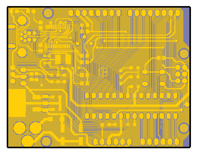
CapExt can import Gerbers, Excellon drill files and DXF-files.

If you want support for other formats, please contact us at info@capext.com

Quickstart examples

CapExt comes with pre-built example projects with matching Gerber files which you can use to quickly familiarize you with how CapExt works, and how to extract the capacitances from your stackup in CapExt. The examples are located in the folder where you installed CapExt, typically C:\Program Files\CapExt\example project\

Back to contents


CapExt projects

Create a new project

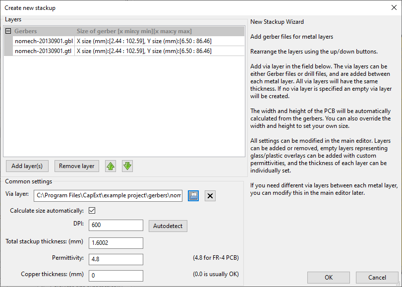
To start a new project, go to File->New Stackup. You will then be presented with the New Stackup Wizard.

Click to magnify.

It is also possible to create a project without going through the New Stackup Wizard, see Project editor Pane.

  • Add Layer(s): Pressing this button will let you select one or more Gerber-, DXF- or drill files to import.

  • Remove Layer: Selecting a layer from the list and pressing this button will remove the layer.

  • up/down: You can also reorder the layers by selecting a layer, and pressing the up/down buttons to move the layer up or down in the stackup.

The last column for each layer is the detected layer dimensions, in either inches or mm depending on the current unit setting. See Change units to metric(mm) or imperial(inches).

  • Via layer: If a via or drill layer is used, specify it here. The via layer will be inserted between each layer. If there is a via from a conductor on one layer connected with a conductor on another layer through a via or drill-hole, the software will detect this and treat both conductors + any connected vias as a single large conductor.

  • Calculate size automatically: The dimensions of the board is automatically detected from the largest dimensions of the imported Gerber files. If you want to override the dimension settings, uncheck the Calculate size automatically box and enter the dimensions manually.

  • DPI: The DPI setting decides which resolution the Gerber-, DXF- or drill files should be sampled at. A too large DPI setting combined with a large board dimension might force the software to spend a very long time importing the files, while providing little to no improvement in the simulation accuracy. For most boards, a DPI in the range 500-1000 is usually sufficient.

    Click Autodetect to have CapExt attempt to automatically set the best DPI.

  • Total stackup thickness: The thickness of the whole stackup. All layers will have an uniform thickness that sums up to total stackup thickness. For more complex layouts, you will need to modify each layer thickness after the Create new stackup wizard, in the Project editor Pane.

  • Layer permittivity is the relative permittivity of each layer. Each layer will be given this permittivity. For stackups with different permittivity for each layer, for example for a touch PCB with an acrylic overlay, you must modify the permittivity later in the Project editor Pane.

  • Copper thickness: If this is non-zero, each non-via layer will have this thickness. This will complicate the stackup later seen in the Project editor Pane, but will not have a significant effect on the simulation time. For stackups where the drill layers are much thicker than the copper, you can usually leave this at 0, but for compact stackups such as wearables or ITO touch surfaces you should specify the thickness here.

All settings in the New Stackup Wizard can be modified later in the Project editor Pane.

CapExt will try to infer the layer type from the layer name, automatically detecting layers that should not be a part of the simulation, such as solder resist layers, giving you the option of ignoring these files.

Silkscreen files and board outline files can be added in order to automatically set the correct board size and adding silkscreen to the top and bottom layers.

Saving a project

To save a project go to File->Save or File->Save As.

Loading a project

To load a project go to File->Open.

Drill file import wizard

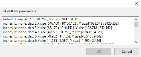
Drill files differ between EDA packages, and CapExt can not always guarantee that it guesses the correct units and formatting of Excellon drill files.

When opening a new Excellon drill file, the best guess for the dimensions of the drill file is displayed, if this dimension looks wrong, or if you see that the drill file is malformed after importing it, you can manually choose how CapExt will import the drill file.

Drill file import wizard

Select the setting which matches either the settings from the EDA package used, or select the option that best matches your existing board dimensions.

DXF import wizard

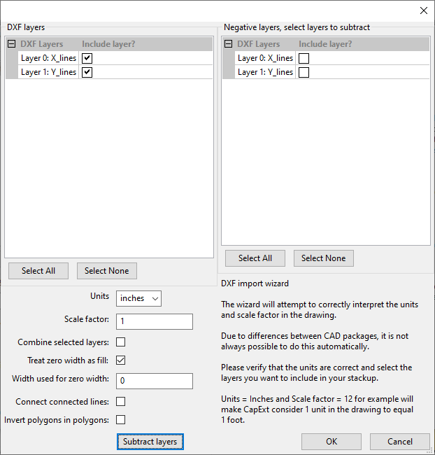
DXF files can contain many layers, and the dimension used in the CAD software used to generate the DXF file is not always saved correctly in the DXF file.

When CapExt detects that you are importing a DXF file, it will present you with the DXF import wizard

DXF import wizard

CapExt will try to deduce the units used and the scale factor from the DXF file, but if you notice that the values are incorrect, you will need to enter scale factor and units manually.

Select the layers you want to import. If you select Combine selected layers, all selected layers will be combined into a single layer. When importing from the Project editor pane this option will always be active. If you are importing the DXF file through the New Stackup Wizard and you uncheck this box, each layer selected will be imported as a separate layer.

If Treat zero width as fill is checked, any zero width lines that forms closed polygons will be filled in. If unchecked, you can override the width for zero width lines with the Width used for zero width-option.

Use Subtract Layers to set layers which will be used as negative layers, subtracting their contents from the other selected layers.

Connect connected lines can be used for cases where polygons are not exported as polygons, but rather as disjoint line segments with common start and end points.

Invert polygons in polygons should be used in cases where you have polygons with internal holes defined by new polygons.

Back to contents


3D/2D view

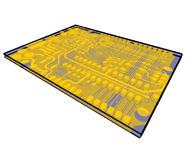
CapExt can display the stackup as either a 3D view or a 2D view. The 3D view is useful for checking that you have the correct ordering of layers or to check the thickness of the layers. Due to the perspective effect, when viewing the stackup head-on in the 3D view, traces directly below each other will not always appear so, in these cases we recommend using the 2D view.

The color of the individual layers are used as an indication of the relative permittivity for that layer, with the color going from clear and transparent for air, to dark blue for relative permittivity higher than 10.0. Electrically conductive traces and vias are yellow.

Navigating in the 3D/2D view

To navigate through the 3D/2D view, simply drag with the left mouse button to drag the board around, scroll with the mouse-wheel to zoom in or out, and drag with the right button to rotate the view.

Navigating with the keyboard

You can zoom in and out with the W/S keys, and you can use the arrow keys to move the view.

Change from the 3D to 2D view

You can freely choose between the 3D view, which is good to verify that the stackup is correct, and the 2D view which is more similar to the familiar view in most PCB CAD software.

To switch between 3D and 2D, go to View->Toggle 3D/2D

Reset view

To reset the 3D/2D view to the standard zoom and position, press View->Reset 3D view.

Back to contents


Project editor Pane

Overview

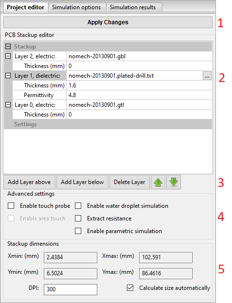
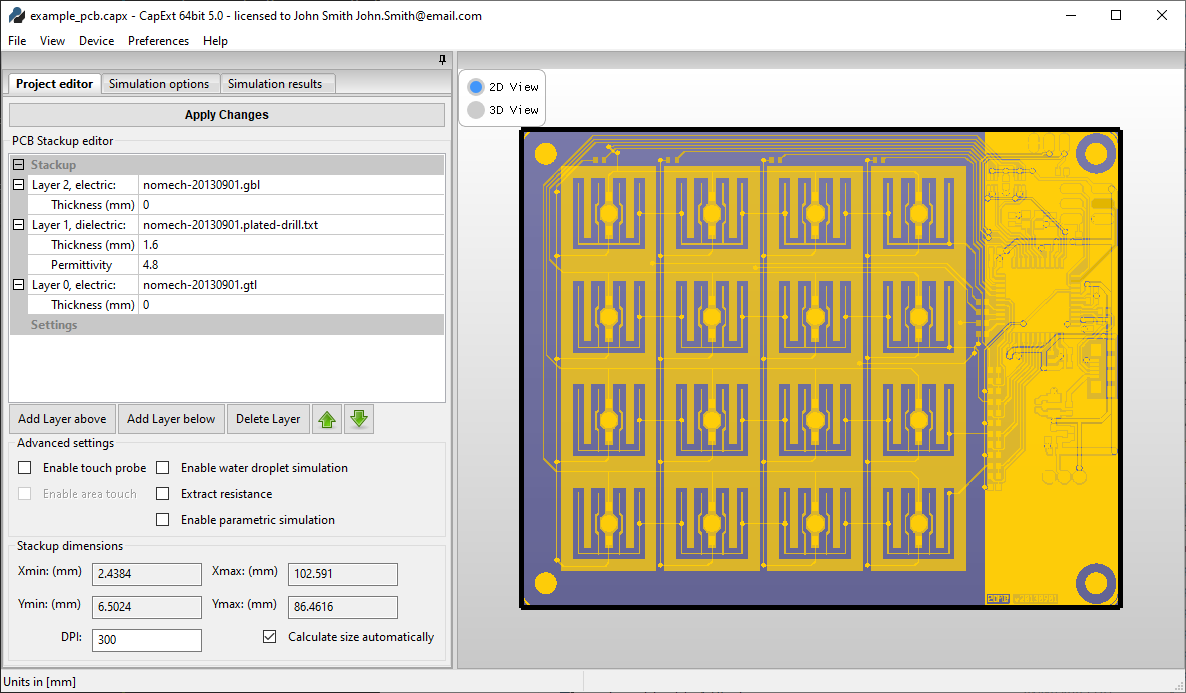
Click to magnify.
  • 1: Apply changes.

  • 2: Select a new Gerber-, DXF- or drill file.

  • 3: Add/remove/move layers.

  • 4: Enable/disable touch functionality, water droplet simulation, resistance simulation and parametric simulations.

  • 5: PCB dimensions, resolution.

Modifying a stackup

All modifications to the current stackup is done in the Project editor Pane.

After modifying the stackup, press Apply Changes. This will update the 3D view of the stackup, and extract all the electrodes from the stackup.

Electrodes which are connected to electrodes on different layers through vias are treated as a single electrode.

Since pressing Apply Changes will change the configuration of electrodes and dielectrics on the board, all electrode names and any simulation results will be lost.

Changing board dimensions or DPI

The dimensions of the layout can be changed in 3 ways:

  • By dragging the board edges in the 3D/2D view: Dragging any edge will mark it red, and will allow you to easily for example crop a PCB in case the Gerber files are larger than the area intended for simulation.

  • By manually modifying the dimensions: X min, Y min, X max and Y max is the coordinates of the board edges, either in mm or inches depending on the units used. Unchecking Calculate size automatically will allow you to enter the dimensions manually.

  • Automatically: If Calculate size automatically is unchecked, checking it again will initiate a scan over all the files to find the maximal board dimensions, the dimension is then set to this maximum.

Adding or removing a layer

Pressing Add Layer above or Add Layer below will add a new layer above or below the selected layer. A layer is built up of a dielectric layer between two electric layers. You can choose to add an electric or dielectric layer. The dielectric layer has a permittivity and a thickness, while the electric layers have not thickness or permittivity. The files set for the electric layers will act as the normal metallic print on a PCB, while the files for the dielectric layers are treated as drill files. If a hole connects to a metallic part on either electric layer, the hole will be treated as a 3D plated through via.

Pressing Delete Layer will remove the currently selected layer. If a dielectric layer is selected with electric layers neighbouring, you have to select which electric layer to delete as well as two electric layers can not touch. The electric and dielectric layers does not need to have associated files, and can be empty.

Moving a layer

Selecting any layer and pressing the up or down buttons will move the layer either up or down. When moving a layer, it will switch places with the next layer in the chosen direction so that every dielectric layer is always surrounded by two electric layers.

Changing layer properties

For dielectric layers, the thickness and permittivity can easily be changed by simply selecting the thickness or permittivity for the layer, and typing in a new value.

Electric layers usually default to 0 thickness, if you type in a thickness higher than 0, you will also get an option to enter the permittivity of the material surrounding the conductive nets in the same plane.

Adding or removing a layer file

To add or change a Gerber-, DXF- or drill file for either an electric or dielectric layer, press the name of the layer, for example "layer 1, dielectric", press the browse button which appears to the far right when the name is selected, and select the new file.

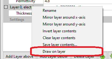
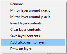
To remove a file, right click on the layer, and select Clear layer contents.

Renaming a layer

Layers can be given custom names by right clicking the layer and select Rename.

Saving a layer

To save the contents of a layer, right click on the layer, and select Save layer contents. This will save the file associated with the layer to the specified location. Any changes done to the layer through Shrink/Grow electrode area is not kept when the layer is saved. Changes done through the layer editor will be. You can also use this functionality to convert between Gerber and DXF.

Mirroring a layer

If a layer is mirrored, right click the layer and choose either Mirror layer around x-axis or Mirror layer around y-axis.

Editing layer contents

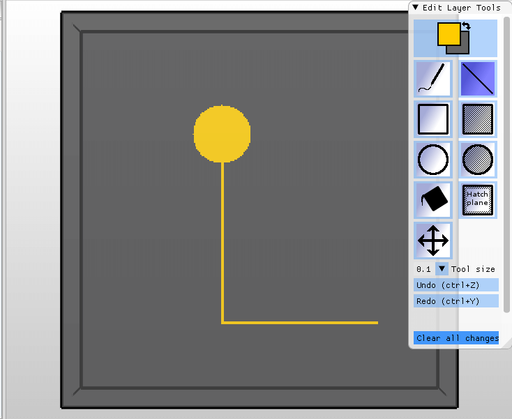
To edit the layer contents without using an external tool, right click the layer, and select Draw on layer.

The layer editor can be used to edit existing layers, for example to optimize sensor designs, add 0 ohm resistors or do other modifications to your layout.

You can also use the layer editor on a blank board to quickly test new sensor designs.

Adding silkscreens to layers

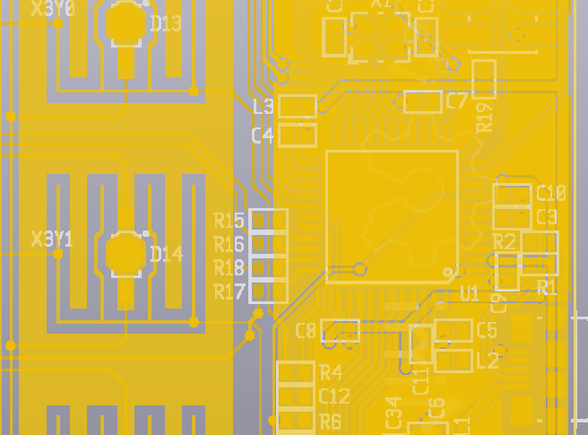
While they are not a part of the simulation, silkscreens can be used to more easily see how PCB designs will look and act after production.

To add a silkscreen to a layer, right click the layer and select Add silkscreen to layer...

The silkscreen can be either in Gerber format or DXF format, and after it is added you can change the color of the silkscreen or remove

The silkscreen color can be changed by modifying the Silkscreen color option in the Stackup editor.

Back to contents


Simulation Options Pane

Overview

Click to magnify.
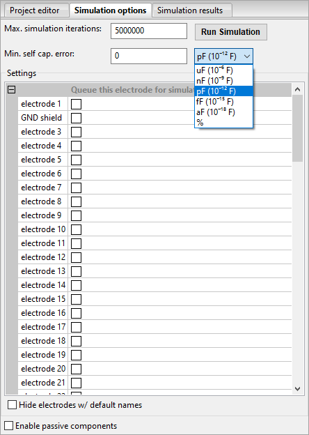
  • Run simulation: Run the simulation

  • Max. simulation iterations: Maximum number of simulation iterations to run, more iterations give better accuracy but also longer run-time

  • Min. self cap. error: The simulation will stop when the required accuracy is met, can be set as a capacitance or a percentage

  • Hide electrodes w/ default names: This option will hide all electrodes which have not been given custom names

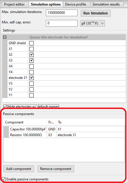
  • Enable passive components: This option will enable the passive component option, allowing you to add resistors and capacitors between nets

Selecting electrodes for simulation

All electrodes detected are given a number and are shown as a list in the Simulation Options Pane. All the electrodes will be a part of the simulation, irregardless if they are selected or not, but only electrodes selected for simulation will have its self capacitance and mutual capacitance to all other electrodes on the board calculated. Therefore, if you want to know the self capacitance of a conductor, or find potential mutual capacitance coupling which might inject noise to a conductor, it is important to select that conductor for simulation.

  • Hovering over an electrode in the 3D view will highlight the whole electrode and display a tooltip with the electrode name next to the mouse.

  • Pressing an electrode in the 3D view will select the electrode for simulation, while at the same time highlighting the electrode in the electrode list.

  • Hovering over an electrode in the electrode list will highlight the electrode in the 3D view.

  • Selecting the checkmark next to an electrode name will select the electrode for simulation.

Any electrodes selected for simulation will be highlighted in green in the 3D view.

Simulation iterations/Simulation accuracy

The more simulation iterations run for each electrode, the more accurate the result will be. The simulation will continue until either the number of iterations has been met or until the calculated self capacitance uncertainty is below the set value.

The total number of simulations is an accumulated number, each electrode remembers how many iterations it has gone through, so if you run a million iterations for an electrode, then select a second electrode, and set the number of iterations to 1000, no iterations will be run for the first electrode, and it will not loose its accuracy, only the second electrode will run for 1000 iterations. If you later set the number of iterations to 2 000 000, the first electrode will be simulated for 1 000 000 iterations, while the second electrode will be simulated for 1 999 000 iterations.

Starting a simulation

To start a simulation, press Run Simulation.

Each electrode selected for simulation will be simulated in sequence. A progress-bar will be shown while the simulation is in progress. You can abort the simulation at any time while still keeping the results obtained so far. If you abort the simulation for an electrode, the next electrode in the queue will be simulated.

Renaming electrodes

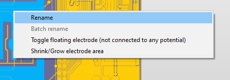
To rename an electrode, for example to mark VCC/VDD/GND or specific pins or touch electrodes, either right click the electrode in either the list or the 3D/2D view and select Rename or left click the electrode name and type in a new name.

You can also rename multiple electrodes at once using Batch rename. To do this, hold CTRL to select multiple electrodes, when you are done, right click one of the selected electrodes and choose Batch rename. The electrodes will be renamed in the order selected, with an increasing number after the name.

This functionality is useful when you have multiple touch buttons or other nets that should be given the same name.

Importing electrode names from an external file

IPC 356 files can be imported to automatically rename all the nets based on the names in your EDA software.

To do this, right click any electrode under simulation options and choose Import electrode names from external file (IPC-356).... After choosing a file, you can select which layer in CapExt corresponds to which layer in the IPC-356 file.

Floating electrodes

Select Toggle floating electrode (not connected to any potential) to enable or disable the selected electrode as a floating electrode

A floating electrode does not have a fixed potential, and this can have an effect on the other nets if the electrode is either large or very close to the net. Each floating electrode will need a separate simulation, so this option should only be used if you are sure that it will have a large effect.

Shrink/Grow electrode area

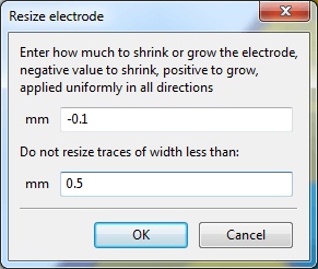
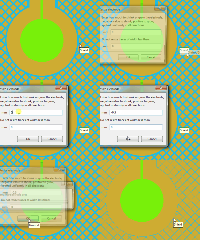
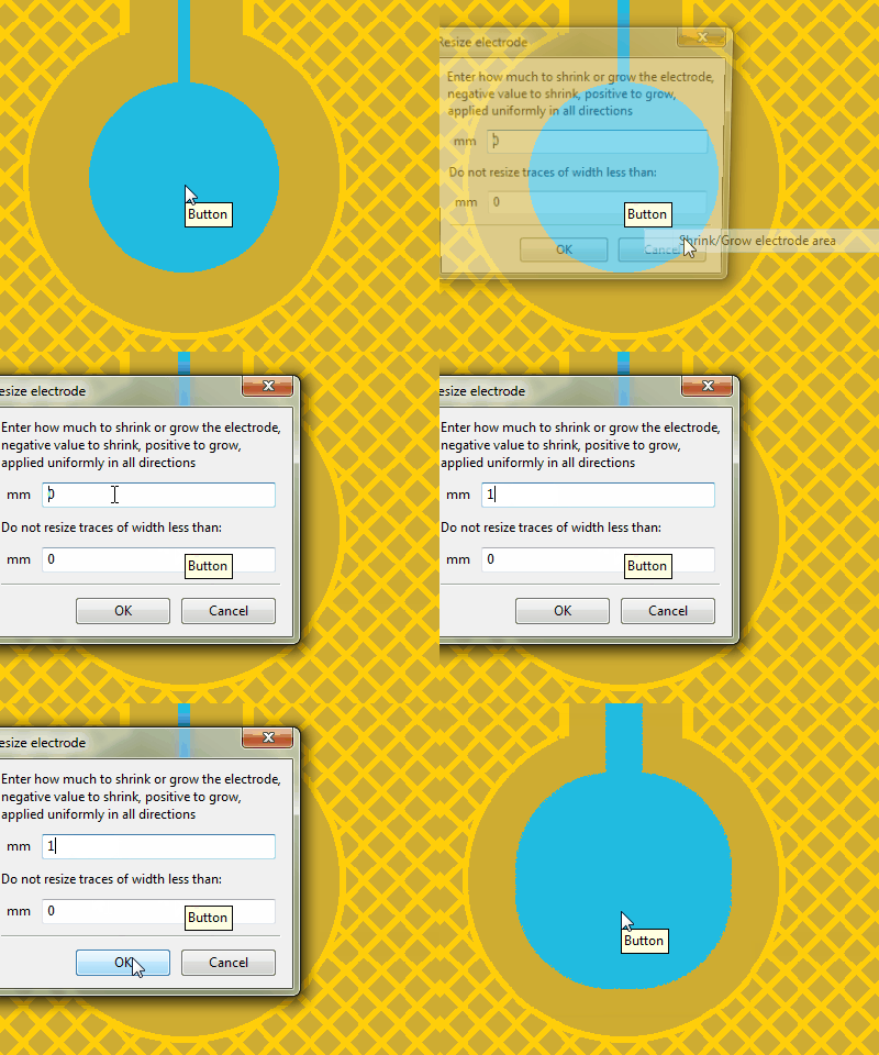
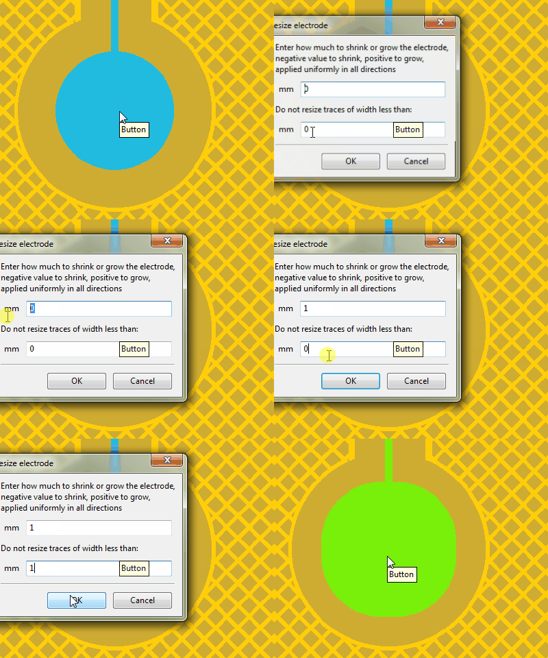
To shrink or grow an electrode, right click the electrode in either the 3D/2D view or in the electrode list and select Shrink/Grow electrode area.

This functionality has been added to ease development of capacitive touch sensors, where you can quickly test the effect of making a sensor smaller or larger, or increasing/decreasing ground hatch % for example.

CapExt will attempt to remove/add material along the edge of the electrode, while ensuring that the electrode does not touch other neighbouring electrodes.


When growing a touch sensor for example, it can be useful to use the do not resize traces of width less than-feature, which ensures that you can grow the sensor while the traces leading up to the sensors are unaffected.


Passive components

Selecting Enable passive components will open the passive components editor:

Click to magnify.

Here you can add resistors and capacitors to your nets.

Resistors will bind nets together so that the calculated capacitance is the capacitance of both nets. The resistance is added to the total resistance calculated when using the resistance extraction feature. You can set the resistance to 0 to emulate a direct electrical connection.

Back to contents


Simulation Results Pane

Overview

Click to magnify.
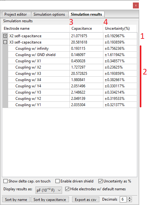
  • 1: Self capacitances.

  • 2: Mutual capacitances.

  • 3: Capacitances column.

  • 4: uncertainty column, note the red numbers in the cases where the simulation needs to run for more iterations to get a better estimate.

Show delta cap. on touch: When enabled, this will show the change in capacitance due to the touch probe instead of absolute capacitance.

Enable driven shield: Open a list where electrodes can be set as driven shields.

Uncertainty as %: Show uncertainty as a percentage of the capacitance.

Hide electrodes w/ default names: This will hide all couplings to electrodes which have not been renamed. Very useful for large and complex PCBs where you do not necessarily care about the mutual couplings to electrodes far away. CapExt will still use these electrodes to calculate the self-capacitance.

Export as CSV: Export the results as a CSV file which can be imported into external programs.

For each electrode selected for simulation, there are two results:

  • Self capacitance: The self capacitance is the total self capacitance seen by an electrode. This is the sum of all the capacitive couplings to all other electrodes in the simulation, also to electrodes not selected for simulaton, and also to the ground placed at infinity.

    The self capacitance and corresponding uncertainty will always be displayed next to the electrode name

  • Mutual capacitance: Pressing the plus sign next to the electrode name will expand the results into a list of mutual capacitances. Here you can see the capacitive coupling from the simulated electrode to every other electrode in the simulation, not just electrodes selected for simulation.

If a result is displayed as 0, then the capacitive coupling is too small compared to the calculated uncertainty, and more simulation iterations must be performed to get a more accurate result.

Hovering over an electrode in the list will color the corresponding electrode in the 3D view dark blue. Hovering over a mutual capacitance result will color the electrode selected for simulation dark blue and the electrode to which the mutual capacitance results belongs will be colored light blue.

By selecting any capacitance on the list and expanding the list, you can press any electrode in the 3D view to find the corresponding result in the mutual capacitance list.

Sorting results

To sort results either by name or by capacitance, press Sort by name or Sort by capacitance. Both the list of self-capacitance and the mutual capacitances for each electrode will be sorted.

Uncertainty

Due to the algorithm used by CapExt, it is possible to get a very accurate estimate of how far the current result is from the accurate physical result. In the results pane, this is represented as an uncertainty value. If the current estimated result is smaller than the uncertainty estimate, the uncertainty estimate is colored red to signify that more simulation iterations should be run if a more accurate result is needed.

The uncertainty displayed is displayed as a standard deviation, meaning that there is a 68% probability that the real result is within [result] ± [uncertainty], and there is a 95% probability that the result is within [result] ± 2x[uncertainty].

Export as CSV

To export the results as a csv file that can be imported into for example Microsoft® Excel, press the Export as csv button. All results available in the simulation results view with the corresponding uncertainty estimates will be exported.

Driven shield

CapExt supports simulation of driven shields. The driven shield functionality is accessed through the simulation results pane.

To configure a net (or multiple nets) as a driven shield:

  • Check Enable driven shield

  • Set the driven shield efficiency. No driven shield is able to follow the sensor potential perfectly, and this value represents how well the shield driver works. This value is usually determined experimentally, but for most cases a value around 80% will give good performance.

  • Select the driven shield electrodes. You can either select them from the list, or select them by clicking the electrodes in the 3D/2D view when the device profile-pane is visible. If you select multiple electrodes, these electrodes will act as a large combined driven shield.


No driven shield


Bottom layer configured as a driven shield
 

You do not need to re-run the simulation after enabling or disabling the driven shield, CapExt will automatically perform the calculations and display the results as if the driven shield is active.

Unless you are interested in knowing the shield capacitance, there is no need to select the shield electrodes for simulation.

Some touch controllers are able to configure the sensors in a way where all sensors not currently being scanned acts as a driven shield. This is supported by CapExt, just select the touch electrodes to also be driven shields, and CapExt will treat them correctly.

What is coupling w/ infinity?

Even for a single conductor alone in an infinite empty space, there is some capacitance, see for example "Does an isolated charged sphere have capacitance?" at HyperPhysics. To model this coupling, a ground box surrounds the stackup in CapExt. The ground-box is extremely large compared to the stackup dimensions to model a ground at infinity. The coupling to this ground box is called "Coupling w/ infinity" in the simulations results.

Back to contents


Touch Simulations

Methodology

Capacitive touch is simulated with a grounded metallic tube as a model for the human finger. While conducting the simulation, CapExt calculates the capacitances with and without the finger probe present, and returns both capacitance matrices.

Configuring the touch probe

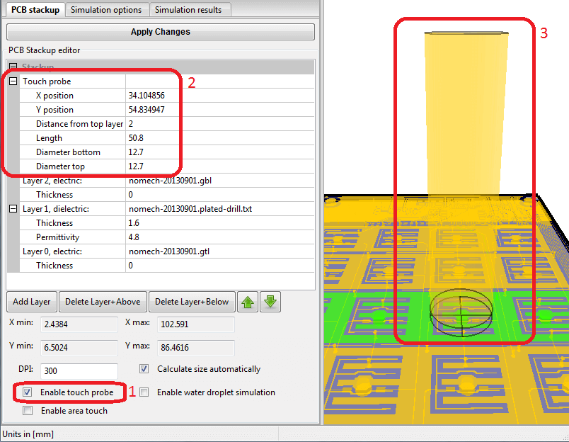
Activating and modifying the parameters of the touch probe is done through the Project editor tab:

Click to magnify.
  • 1: Enable touch probe. Check this box to add a touch probe to your stackup.

  • 2: Physical dimensions and position of the touch probe.

  • 3: Visual representation of the touch probe. Click and drag to move the touch probe.

Remember to press Apply Changes after reconfiguring the touch probe.

Interpreting the results

Click to magnify.
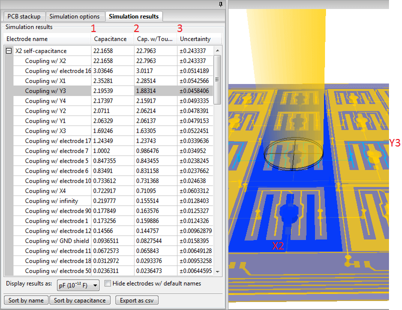
  • 1: Capacitance without the finger probe present.

  • 2: Capacitance with the finger probe present.

  • 3: Uncertainty of the measured capacitance with the touch probe present.

In the results above, we can see that the mutual capacitive coupling between X2 and Y3 is ~2.2pF before the touch event, and ~1.9pF after, with an uncertainty of ~0.046pF.

When simulating capacitive touch, you are usually interested in the change in capacitance rather than the absolute value of capacitance. In order to ensure high quality of your results, you should check that the reported uncertainty is much less than the difference in capacitance due to the touch. If that is not the case, increasing the number of iterations in steps of 10x until the uncertainty is within acceptable limits is recommended.

Advanced settings

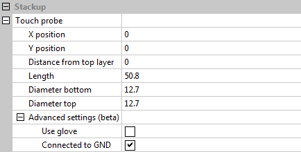
You can enable additional experimental touch features under the Advanced settings (beta) category:


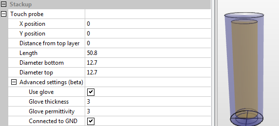
Use glove

When activated, the touch probe will be surrounded by a uniform layer of chosen thickness and permittivity to simulate a glove around the finger.

Finger with glove

Connected to GND

If you uncheck this box, an extra simulation step will be performed that allows you to later select if the touch probe should be:

  • Grounded: This is the same as not unchecking the box, the touch probe will be connected directly to a fixed potential as if grounded.

  • Floating: The touch probe is not connected to any potential, i.e. it is left floating. The change in self capacitance due to the touch probe is typically lower in this mode.

  • Probe to GND through cap: The touch probe is connected to a fixed potential through a configurable capacitor. This is to emulate a typical physical touch probe.

These settings are accessed through the Simulation Results pane after the simulation has finished.

Back to contents


Area Touch

The area touch functionality is similar to the touch functionality, but instead of simulating a single touch by a finger or stylus, you can simulate many independent touches across an area of your board.

This can be used to find the area around a touch button which will report as a touch, or to check the linearity of a slider, wheel or touch screen.

Configuring area touch

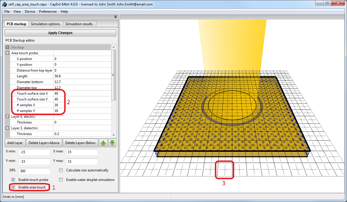
To enable area touch, in the Project editor pane first click Enable touch probe and then click Enable area touch.

Click to magnify.
  • 1: Enable area touch, clicking this checkbox will activate area touch

The settings for area touch mirrors the settings for a normal single touch simulation, the X and Y positions sets the center of the area over which the touch probes will be spread, and distance from top layer, length, diameter top and bottom is common to each touch probe in the area touch simulation.

To move the area, either change the X Y positions manually, or click and drag the touch probe at the center of the touch area in the 2D/3D view.

  • 2: Settings specific for area touch

    • Touch surface X/Y: The size over which the area touch probes will be spread

    • # samples X/Y: The number of touch probes that will be simulated in the X and Y directions

  • 3: The grid shows where each touch will be simulated, a touch probe will be simulated at the center of each cross

Once area touch is configured, press Apply Changes to finalize the setup.

You can now run the simulation as you normally would.

Viewing the results of an area touch simulation

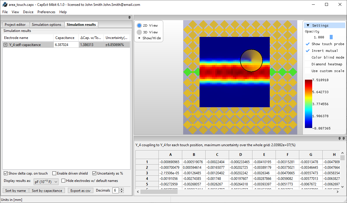
After the simulation is done, you can click on any electrode in the Simulation results pane to see the results of the area touch simulation.

Click to magnify.

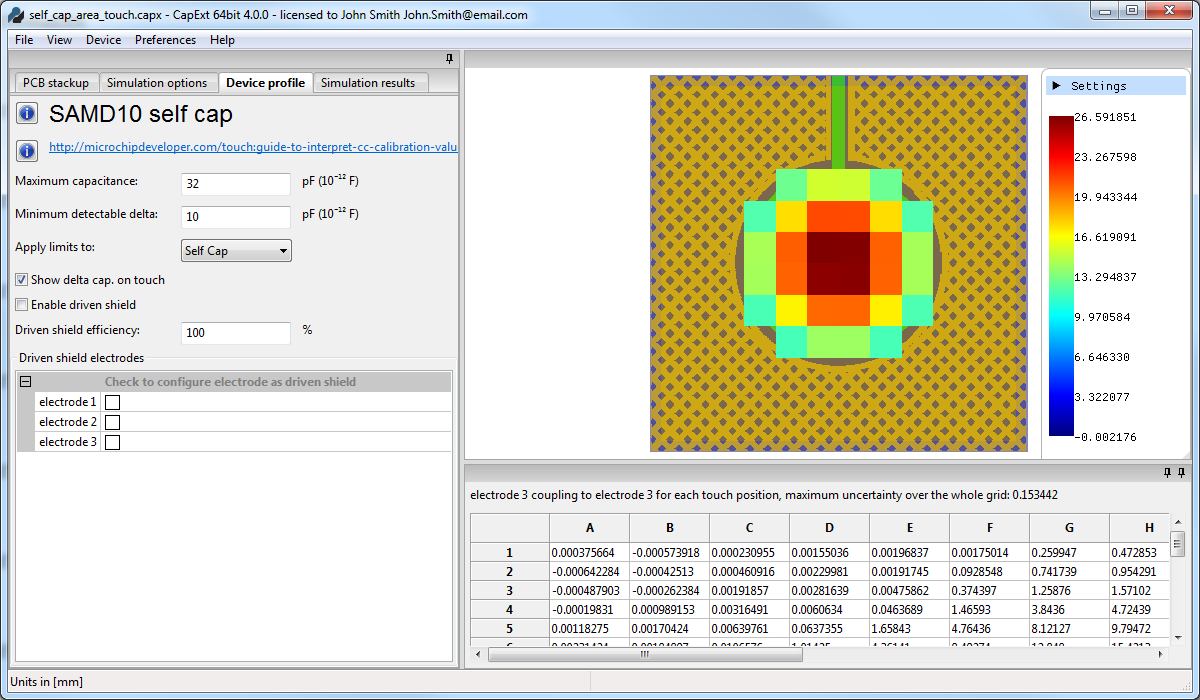
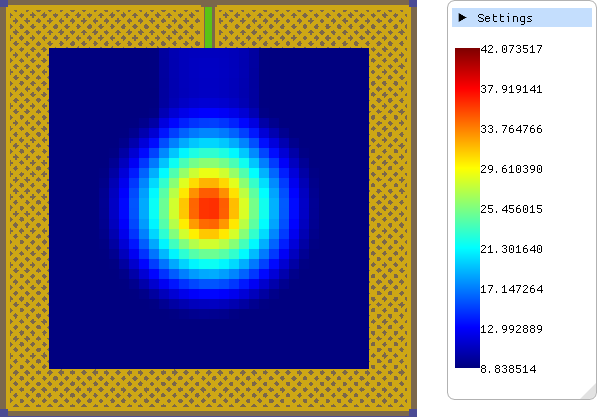
In the 2D/3D view you will see a heatmap indicating the change in capacitance when the touch probe touches the center of each point in the heatmap. The scale on the right-hand side shows what capacitance value each color corresponds to.

At the bottom of the screen you can view the exact capacitance for each square in the area touch simulation. the element A1 corresponds to the upper left corner, with letters running from left to right, and numbers running from top to bottom.

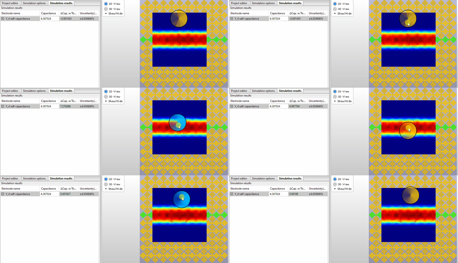
The capacitance next to the name of the electrode is the self-capacitance when not touched, and next to that is the self-capacitance for the current probe position.

You can drag the touch probe around inside the selected area to view the corresponding capacitance for each touch position as if the simulation was a normal single touch simulation.

Selecting new probe positions

To view mutual capacitances, press the small + next to the electrode name, and click on the electrode which you want to see the mutual coupling to.

Area touch and mutual capacitance

You can also view the sum of the area touch results from either multiple self-capacitance simulations or multiple mutual capacitance simulations. This can be very useful to ensure that you have good linearity on touch screens, sliders or wheels. To sum results, CTRL-click the results in the left pane that you want to sum.

Adding up several mutual capacitances to see linearity
Configuring the area touch scale

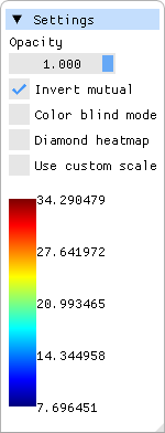
Pressing the Settings button at the top of the scale will show configuration options for the scale.

Configuring the scale

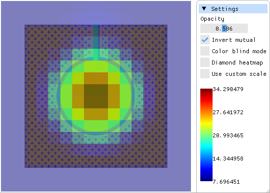
Opacity: How transparent the heatmap should be, setting it to 0 will hide the heatmap.

Opacity = 0.5

Invert mutual: Since changes in mutual capacitance due to touch are normally negative, CapExt will by default invert the color scale when viewing mutual capacitances, if this is unwanted, uncheck this box.

Color blind mode: This changes the color scale to one that is easier to read for color blind people.

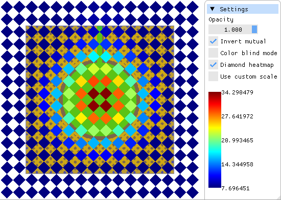
Diamond heatmap: Change the heatmap to a version where there are gaps between each square so that you can simultaneously view the layout and the heatmap without reducing the opacity.

Diamond heatmap

Use custom scale: Normally the min and max values in the scale are the min and max values of all the grid points in the results of the area touch simulation, checking this box will allow you to change the minimum and maximum values.

Device profiles and area touch

You can combine the area touch functionality with a device profile to either check the effect of a driven shield on the touch sensitivity, or to see how large an area will report as touch for a chosen sensitivity.

Minimum detectable delta tuned to give the optimal touch response
Plotting a touched path

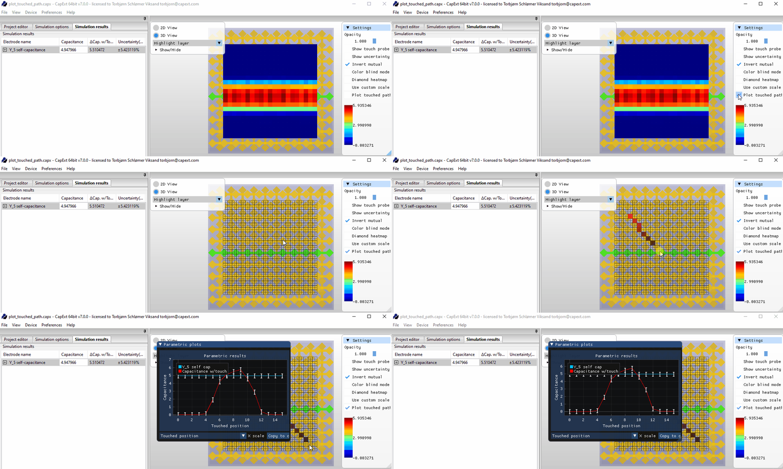
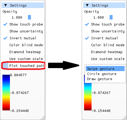
Using the plot touched path feature you can easily see how the simulated circuit would react to gestures.

Clicking the plot touched path checkbox will allow you to choose between plotting a swipe gesture, a circle gesture, or a custom gesture.


After selecting one of these options, you can draw a path on the simulated area, after which CapExt will plot the touched path.


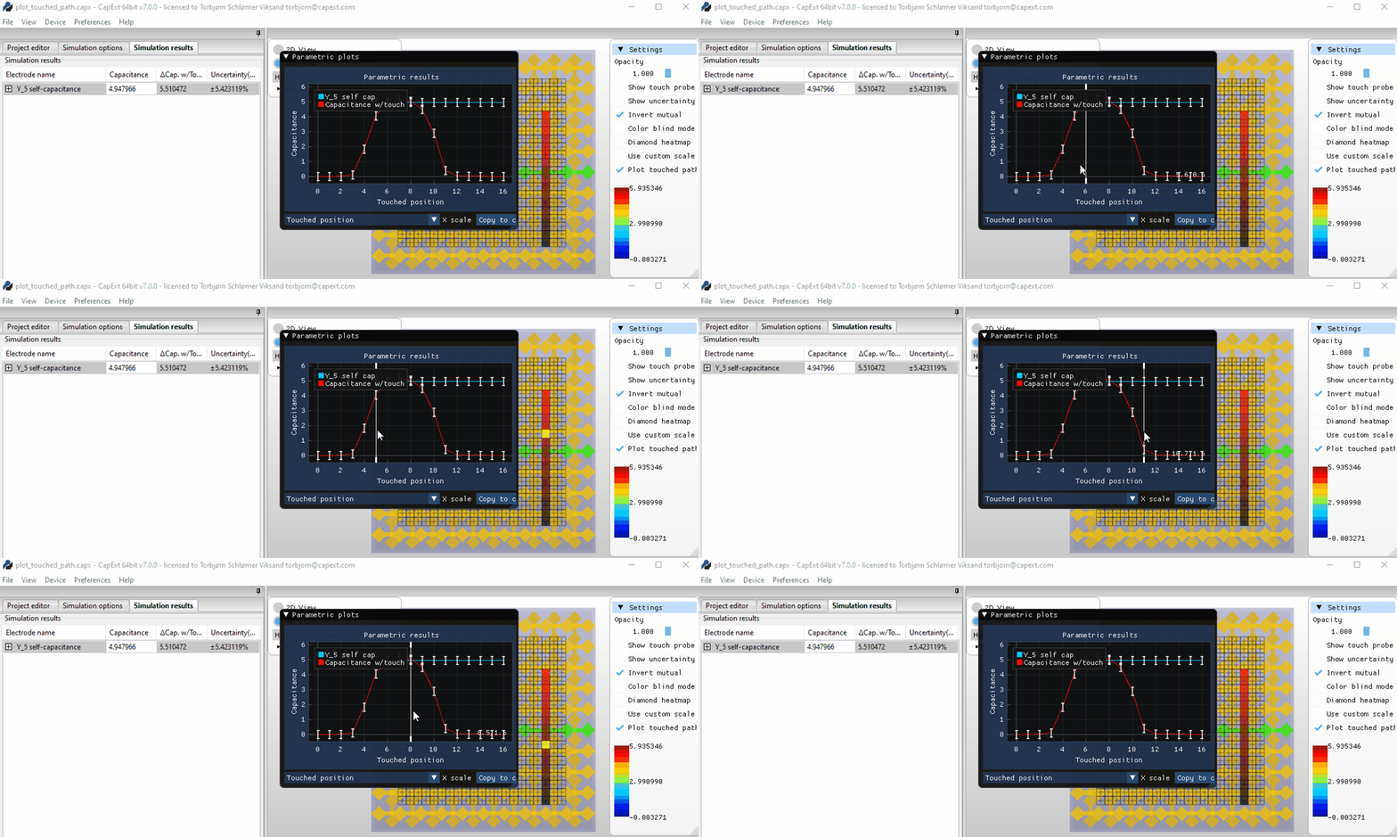
Hover over any position in the plot to see the corresponding pnysical touch position.


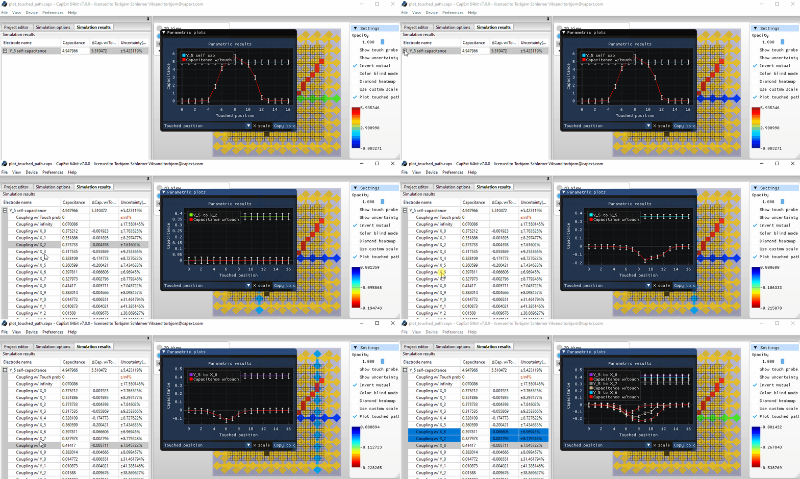
You can also select different electrodes, or even multiple electrodes to see how different parts of the circuit reacts to the touch gesture.

Simulation time and area touch

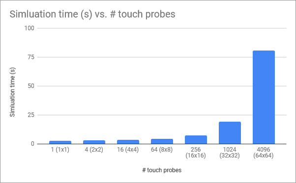
The area touch functionality has been designed to be fast and easy to use, and the simulation time does not scale linearily to the simulation time of a single touch. You can simulate up to thousands of touches in just a few minutes.

In the following benchmark, a self-capacitance button on a somewhat complicated board (~250 electrodes) is simulated with a default configuration for the area touch probes, the area over which the touch probes are distributed is 100x100mm centered above the button. The simulations are performed on a desktop computer with an Intel(R) i7-4790K CPU with 16 GB RAM.

Simulation time vs # touch probes

Simulation time will vary depending on the required uncertainty, distance between each individual touch probe in the area touch simulation, how complicated the layout is and the machine used to perform the simulation.

Back to contents


Resistance extraction

CapExt can extract the resistance of any net. To make this feature easy to use, CapExt automatically finds the two most distant point on the net, and calculates the resistance between these two points.

Configuring resistance extraction

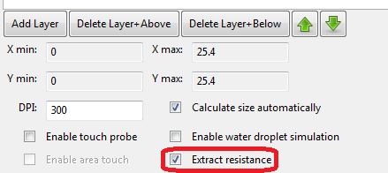
To enable resistance extraction, check the Extract resistance checkbox at the bottom of the Project editor-pane:

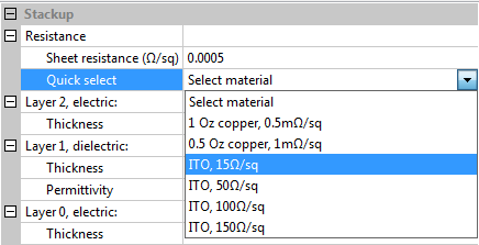
In order to get accurate resistance values, you must input the conductivity of the material used.

Either select the material from the Quick select-menu, or input your own value for the sheet resistance.

Any electrode selected for capacitance extraction will automatically be queued for resistance extraction.

If custom endpoints are needed for the resistance extraction, you can right click the electrode when the Simulation Options pane is open and click Choose endpoitns for resistance extraction to select custom endpoints.

Resistance extraction results

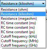
After the simulation is done, the resistance will be displayed as a new column in the Simulation results-pane.

You can also choose to see the RC time constant, calculated as resistance * capacitance, or the cutoff frequency calculated as 1/(2pi*RC).

Setting a non-zero value for Series R (Ohm) will add this resistance to all calculated resistance values. This can be useful in for example touch designs where a fixed series resistance is often used to reduce noise.

Back to contents


Device profile

Overview

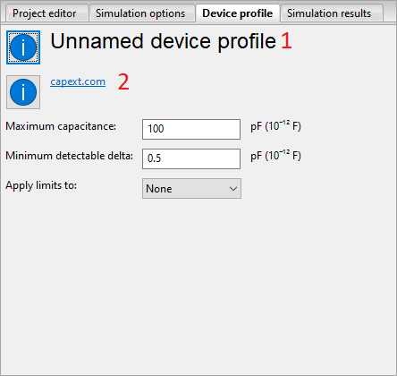
Device profiles contains the parameters you are interested in when using a touch controller.

Click to magnify.
  • 1: Device name, press the button to the left of the name to change the name.

  • 2: URL to documentation for the device, press the button to the left of the URL to change the URL.

  • Maximum capacitance: The maximum capacitance that the device supports.

  • Minimum detectable delta: The minimum capacitance change required for the device to report a touch.

  • Apply limits to: Here you can select if the limits above should be applied to self capacitance, mutual capacitance, both self and mutual capacitance or none. If the results are outside the limits, the result will be colored red in the simulation results pane

CapExt comes with a number of touch controllers from some select vendors, but if your chosen touch controller is not in this list, you can easily create a new device profile for your controller.

Enabling or disabling device profiles

Device profiles can be enabled or disabled by selecting Device->Enable/disable device profile.

Saving a device profile

If you want to reuse a device profile for multiple projects, you can save the device profile by selecting Device->Store.

Loading a device profile

To load a custom device profile, select Device->Load->Load from file.

If you want to load a preconfigured device profile, select Device->Load->Vendor. and navigate to the device you are using. These device profiles are stored in [CapExt installation folder]\Vendor, if you want your own devices to appear in this list, store the device profile in this folder.

Back to contents


Water droplet simulation

Overview

CapExt can simulate conditions where the design is subjected to water. This is very useful when doing touch simulations where you want to know how your design performs under different wet conditions.

The water droplet simulation simulates a covering of the top layer with water droplets. You can configure the droplet parameters, and choose between directly positioning the droplets yourself, or using the Randomize droplet positions functionality where CapExt will simulate thousands to millions of different droplet positions and return the average of all the simulations.

Enabling the water droplet simulation

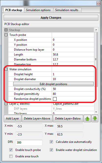
In the Project editor-pane select Enable water droplet simulation. A new item called Water simulation will be added to the stackup pane:

Water simulation

Configuring the water droplet simulation

The default setting corresponds to a light coverage of rain. You can control the water droplet simulation with the following parameters:

  • Droplet height: The thickness of the droplets in the z-direction.

  • Droplet diameter: The width of the droplets.

  • Edit droplet positions: Pressing this button will activate a mode where you can manually place, move and delete droplets.

  • Droplet conductivity (%): The electrical conductivity of the droplet, 0% will represent pure distilled water, while 100% will represent water with the conductivity of a metal (extremely salt water for example).

  • Droplet permittivity: The relative permittivity of the liquid, water is typically at around 80 at room temperatures, but if you want to simulate another liquid, such as oil for example, you can change this value.

  • Randomize droplet positions: Checking this box will randomize the droplet positions.

To perform a simulation with water droplets present, either place the droplets manually or select randomize droplet positions and press Apply changes, and run the simulation as you normally would.

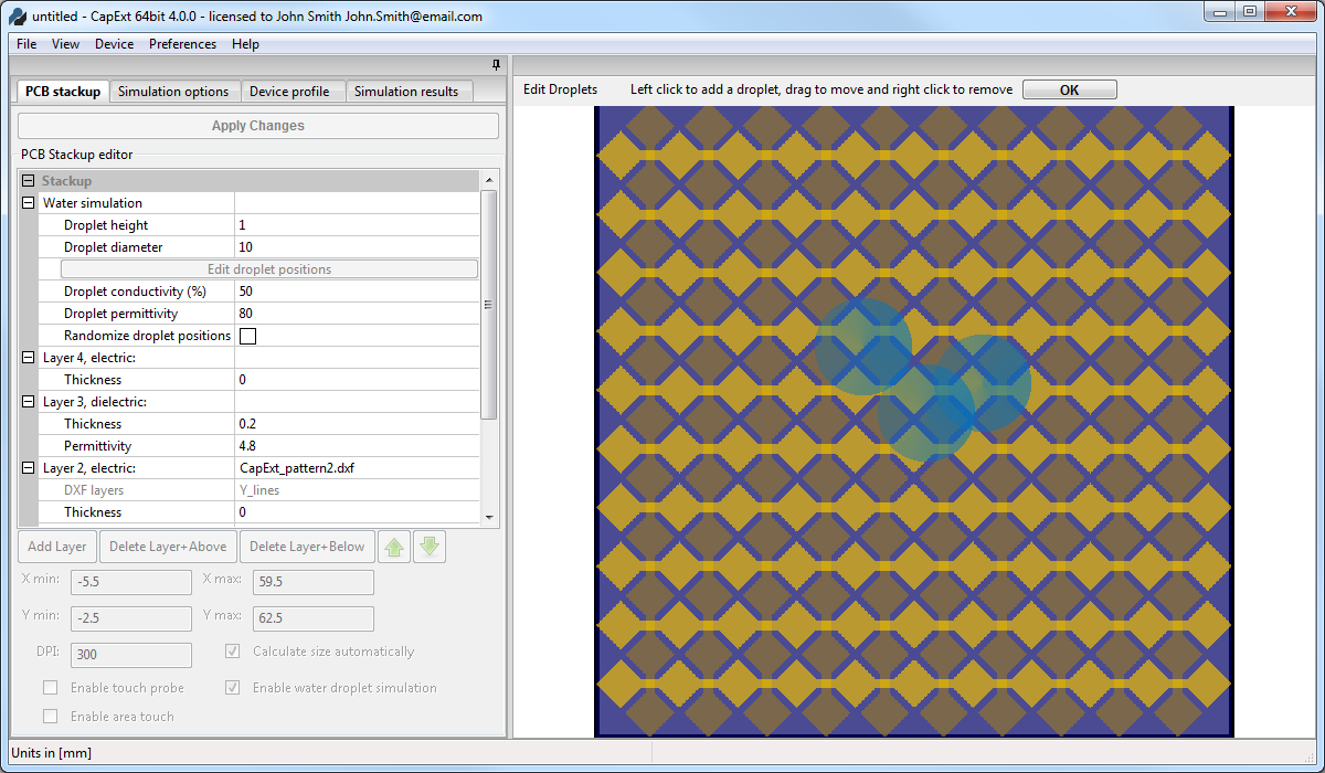
Edit droplet positions

Pressing Edit droplet positions will enable an editor that allows you to click anywhere on the board to add a new droplet, drag existing droplets to move them and right click to remove droplets

Droplet editor

Either click OK or anywhere on the Project editor pane to exit the droplet editor.

Randomize droplet positions

If you activate randomized droplet positions, Edit droplet positions will be replaced with Droplet coverage (%) which lets you specify the area of the top layer which is covered by droplets. If necessary, droplets will overlap and combine into larger droplets to fulfill the area criteria.

CapExt will create an animated overlay over the top layer to represent the water droplets. The height and width of the droplets corresponds to the size used in the simulations, and the coverage of the droplets will be approximately what is used by the simulation, but the exact position of the droplets will be randomized many times over during the simulation.

Water droplets with driven shield

To hide the water droplet overlay, select View->Show/Hide water droplets

Simulation results with water droplets

When the water droplet simulation is active, CapExt will perform two simulations simultaneously, one with water, and one without water. This lets you easily see which effect the droplets have on your layout, and compare this with the capacitances when no water is present.

In the simulation results pane, you can toggle between viewing the results without droplets, with droplets or droplets - no droplets

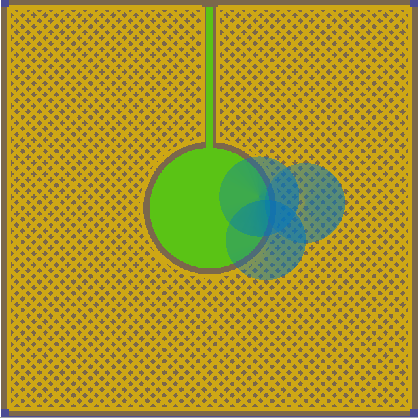
The droplet pattern used

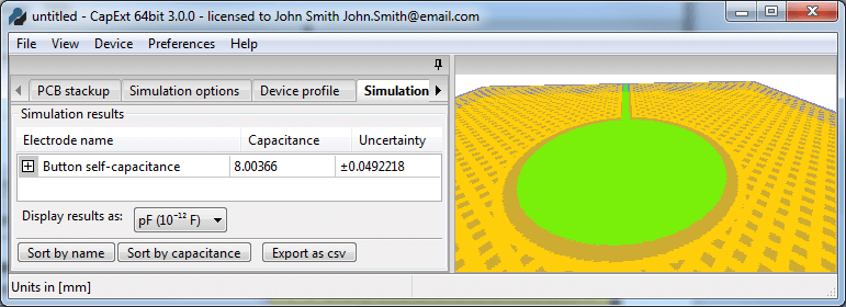
Without droplets: Display the capacitances when no droplets are present:

Without droplets

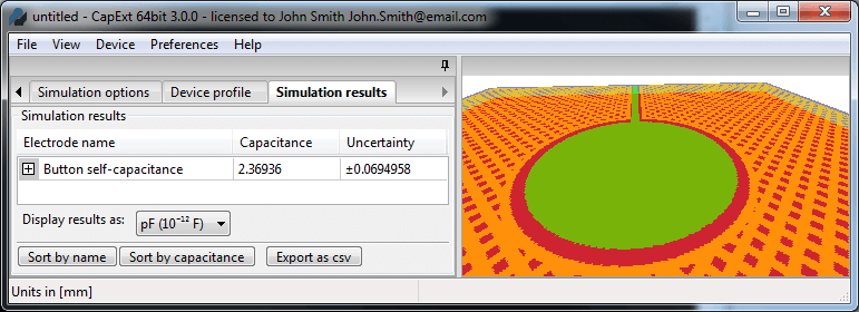
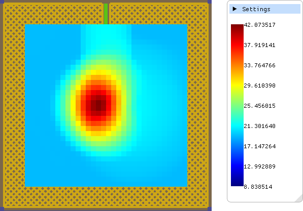
With droplets: Display the capacitances when droplets are present, we can see from the following picture that the self capacitance has increased due to the droplets placed nearly directly over the capacitive button:

With droplets

Droplets - no droplets: This setting will display the difference between the results with water and the results without water, can be very useful if you are interested in detecting false touches due to moisture:

Droplets - no droplets

Combining area touch and water droplet simulations

The area touch functionality can easily be combined with the water droplet simulation to get an intuitive graphical overview of how touch sensitivity across different x-y positions are affected by water droplets.

The screenshots below use the same droplet pattern as in the preceeding section.

Area touch without droplets Area touch with droplets

From the screenshot above, we can conclude that the droplets would probably trigger a false touch, and the sensitivity of the button when the droplets are present on the right side of the button will change the sensitivity pattern significantly.

Back to contents


Pattern generator

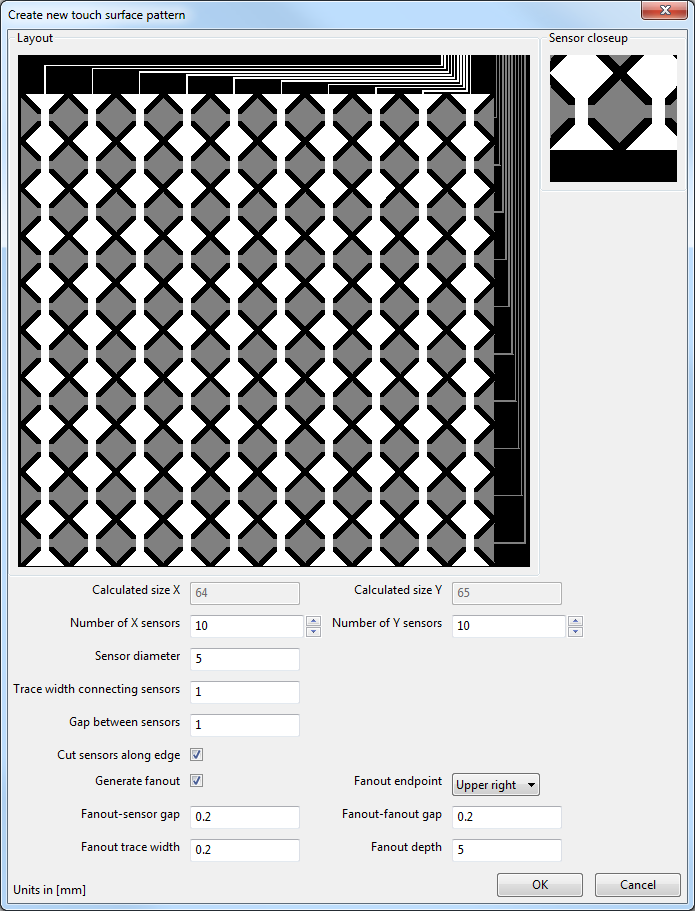
CapExt comes with a tool to generate new touch screen and touch surface patterns. The patterns are based on a standard diamond pattern, if you would like to see other patterns in the pattern generator, please contact us.

To generate a new pattern, go to File->New Pattern->Diamond Pattern (Touch Screen/Surface).

Using the pattern generator

Pattern generator
The largest image shows the complete pattern, while the frame in the top right corner shows a close up on how each sensor element will look. Both images will update as you change the pattern parameters.

Once you are done configuring your pattern, click OK and the new stackup wizard will open with your pattern pre-loaded, configure your stackup and press OK again.

You can now use the pattern as if you loaded it from an external file. The X- and Y-lines will be automatically named as such.

If you want to save your pattern to edit in another program, or if you want to use it to manufacture a touch screen or surface, right click one of the layers containing the pattern in the PCB Stackup Pane and select save layer. The pattern will be saved as a DXF-file with one layer for the X-lines and one layer for the Y-lines.

Back to contents


Parametric simulations

Parametric simulations allow you to vary one or more parameters across multiple simulations. The results can be viewed per simulation, or as a plot of all the simulations.

Using parametric simulations

Click Enable parametric simulation in the Project editor pane to enable parametric simulations.

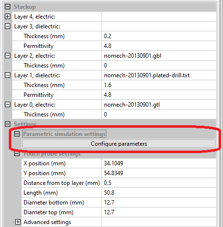
This will open the Parametric simulation settings option in the Stackup Editor.

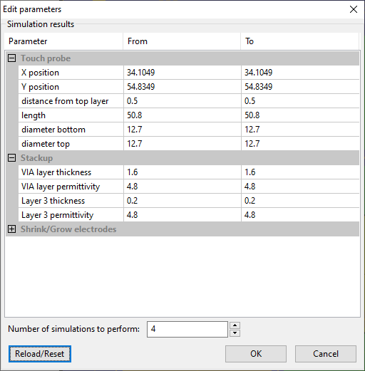
Click Configure parameters to edit which parameters to vary across how many simulations.

Change From or To for any parameter to have CapExt linearly interpolate the parameter between these values over the chosen number of simulations.

If changes have been made to the stackup since you last edited the parameters, you need to press Reload/Reset to update the list of parameters.

When you are done, you can press OK followed by Apply Changes and Run Simulation to start the simulations.

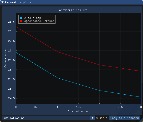
Clicking on a result in the Simulation results-pane will now show a graph of the result across the simulations performed;

You can also change the X scale to the parameter varied, for example layer thickness or touch probe position, or copy the results to the clipboard for easy plotting in external software.

To see the exact results for each simulation, you can select which simulation is currently displayed in the results list by changing the Parametric simulation no option. The 3D view will also update to show the state of the chosen simulation.

Back to contents


Miscellaneous

Change units to metric(mm) or imperial(inches)

The current unit setting can always be seen in the info-bar in the lower left corner of the application. To switch between Units in [mm] and Units in [inches], go to View->Units.

Show/Hide layers

Individual layers can be hidden by going to View->Show/Hide Layers. This will open a dialog where you can individually turn layers on or off. This is useful if an electrode is below another electrode, making it both hard to see and hard to select.

To show all layers again, select View->Show All Layers.

Batch simulations and scripting

CapExt has extensive batching and scripting functionality. Common use cases are:

  • Running multiple simulations overnight.

  • Automated testing of different parameters, such as the thickness of the substrate or overlay.

  • Complex touch simulations. For example, you can set up a stackup with a touch probe on one end of the board, and using the scripting interface you can move the finger across the board, performing simulations and storing the results as the finger moves, simulating a swipe event.

The scripting interface is invoked by calling CapExt with a script as a parameter. For information on the different commands available, pass the parameter "--h" to capext from the command line. Please contact us if you would like to have access to additional features of CapExt througth the scripting interface.

Back to contents


Pro Features

These features are only available to users with a license to CapExt Pro, to upgrade your license or request a trial of CapExt Pro, please contact sales@capext.com

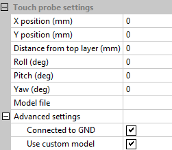
Model Touch Probe

With the model touch probe you can use a custom 3D model in place of the standard cylindrical touch probe.

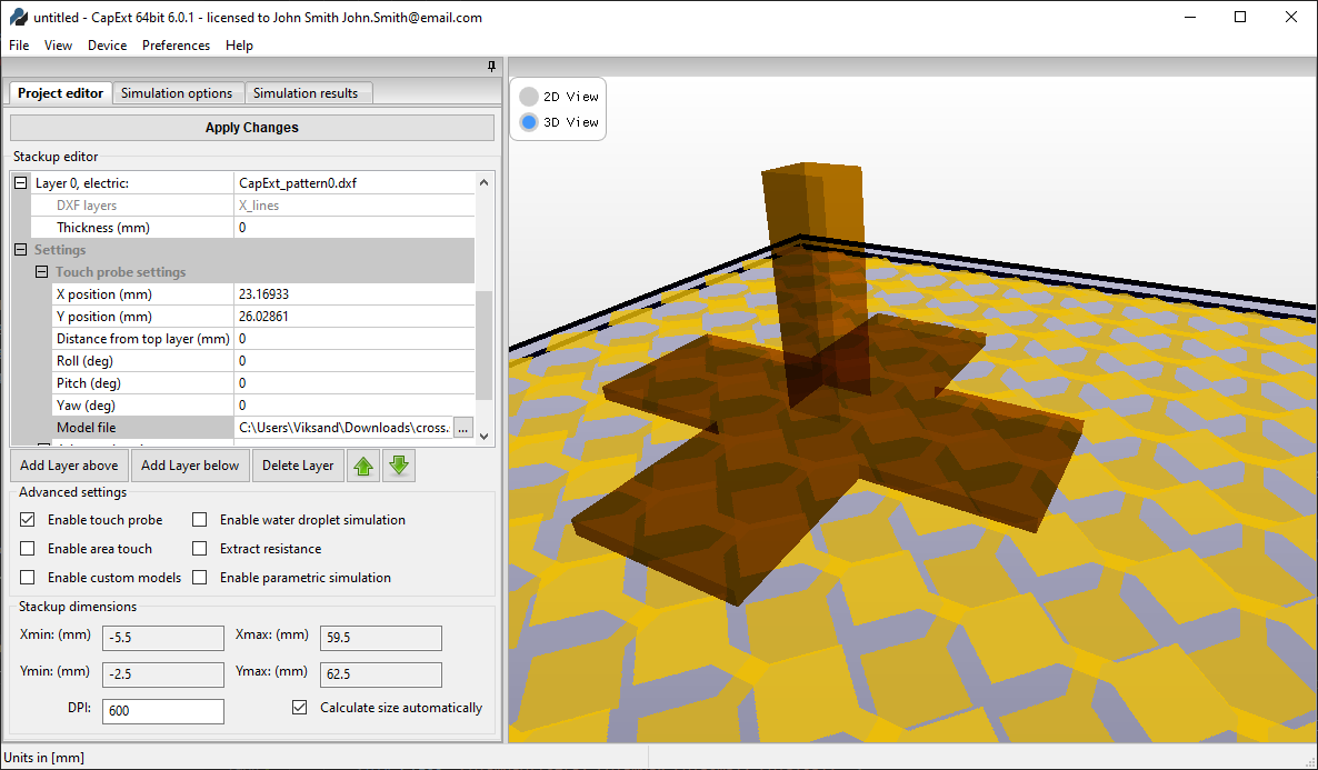
To activate model touch probe, enable a standard touch probe, expand Advanced settings for the touch probe and select Use custom model.

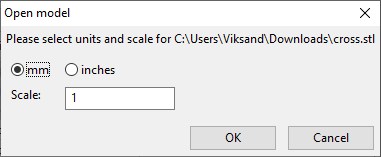
Import an STL model file by clicking Model file. You will be prompted to select if the unit in the model file is inches or mm, and if you would like to scale the model.

Once the model is loaded, it will appear in CapExt as a touch probe that can be moved around like a normal touch probe.

You can rotate the 3D model by modifying the values for roll, pitch and yaw.

Additionally, you can use parametric simulations to simulate the touch probe moving or rotating over the stackup.

Custom Models

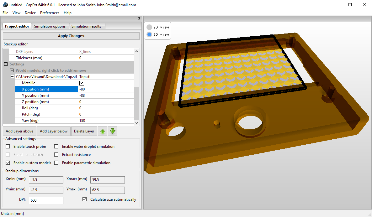
Custom models allow you to use custom 3D geometries in addition to the flat stackup. This can be used to simulate complicated features such as enclosures or plastic or metallic elements in proximity to the stackup.

To activate custom models, click Enable custom models in the Project editor pane.

This will add a new line to Settings in the Stackup editor labeled World models, right click to add/remove.

Right click this line and select Add model... to add a model.

You can have several models in the same project, and they will all appear under this heading. To remove a model, right click it and select Remove this model.

As with the Model Touch Probe each model can be independently moved and rotated.

To set a model to be dielectric instead of metallic, uncheck the Metallic checkbox and enter a permittivity value. In order to be dielectric a model have to have well-defined normals and be watertight. CapExt will check if this is the case when the checkbox is clicked, and display a notification if any issues are detected.

3D boxes

3D boxes can be used to quickly build up simple or complicated structures, such as metallic keys or glass overlays that can not be constructed as a part of the stackup.

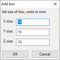
To add a 3D box, right click World models and select Add simple 3D box.... This will open a dialog where the dimensions of the box can be set.

After clicking OK a box will be added, acting just like a custom 3D model that can be moved and rotated freely.

3D springs

Springs are commenly used as a conductor between a PCB and a touch sensitive surface.

3D springs in CapExt are used the same way. They will automatically connect electric layers below and above them to act as a single large electrical net.

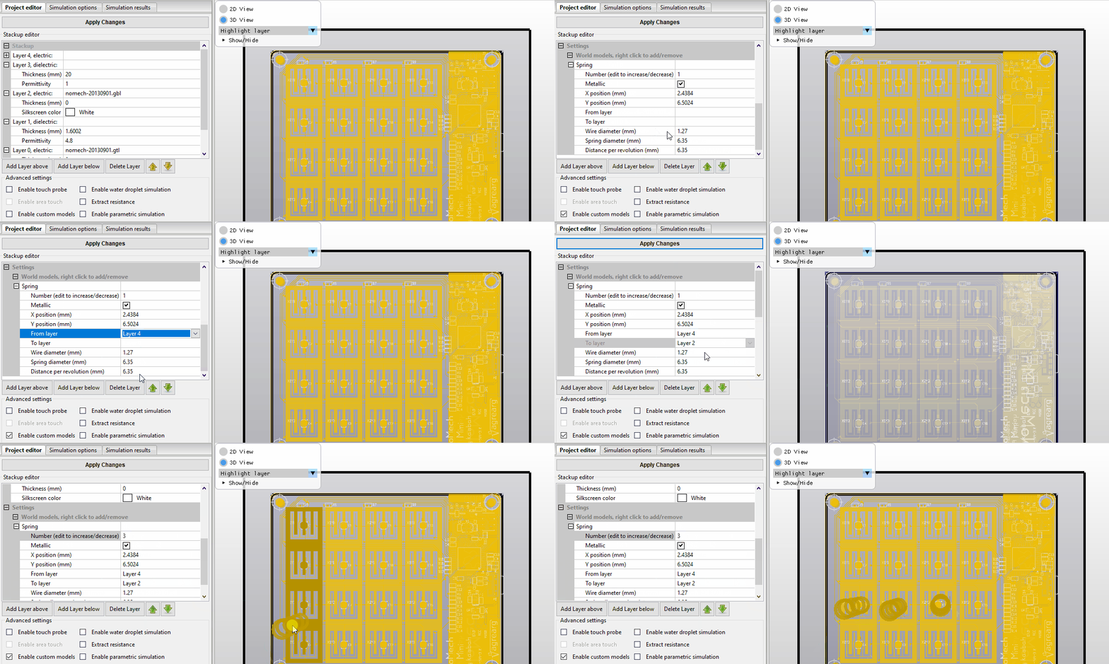
To add a 3D box, spring click World models and select Add spring.

Springs with the same start and end layer and the same dimensions will be grouped together.

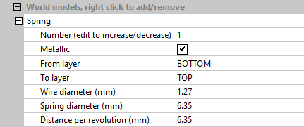
  • Number of springs: Increase or decrease this number to add or remove springs. New springs will be added to the layout and can be dragged around in the 2D/3D view using the mouse.

  • Metallic: The spring is a 3D model, and as other 3D models it can be set as either conductive or non conductive.

  • From layer/To layer: The springs will be between these two layers.

  • Wire diameter: Diameter of the metallic wire in the spring.

  • Spring diameter: Diameter of the spring.

  • Distance per revolution: Distance between each revolution of the spring wire..

Layers that will be elctrically connected by the spring will darken in color as you move a spring around.

Back to contents